
Amkor Technology, one of the world’s leading providers of outsourced semiconductor packaging and testing services, increased its investments in research and development in 2021.
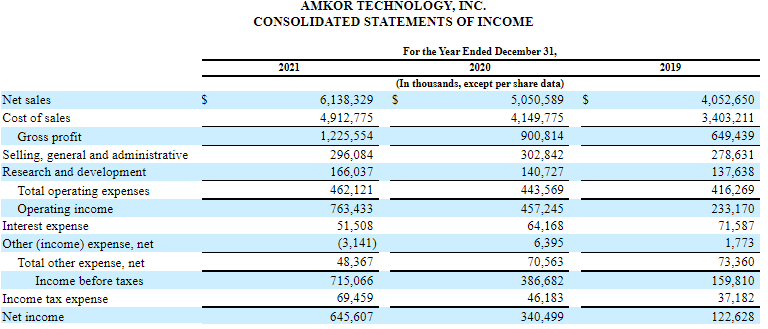
The company invested 166 million dollars in this concept, which represents a growth of 18% year-on-year and 20.6% over 2019.
Its research and development employees are located in South Korea, the United States, Portugal, and elsewhere in Asia.
As of December 31, 2021, the company had approximately 550 employees engaged in research and development activities.
In general, Amkor’s research efforts are focused on developing new packaging solutions and testing services, as well as improving the efficiency and capabilities of its existing production processes.
The company believes that technology development is one of the keys to success in the semiconductor test and packaging industry.
By focusing its research and development on its customers’ needs for innovative, higher-performance, lower-cost packages, the company gains opportunities to enter markets early, successfully compete for new products, and promote its new package offerings as leading technology in the industry.
One of its top priorities is to develop highly integrated modules, such as DSMBGA packages, to reduce material and processing costs and minimize the form factor for 5G wearable and mobile devices.
Amkor investments
Another major focus area is the development of wafer-level packages for larger chips.
These wafer-level chip-scale packages and WLFO packages are increasingly the preferred package type for many applications in IoT and mobile devices, including power management integrated circuits (PMICs), display controllers, and antenna products in package.
Amkor is also developing new applications for the automotive market using new and existing package technologies as higher performance compute and sensor content are used to support new automotive features including ADAS, infotainment, optical sensors and electric vehicles.
Another focus for development is multi-die embedded solutions, including multichip modules and high-density WLFO solutions, which enable package-level integration of different types and levels of silicon technologies for data center, network, and computing applications. high performance computing.
This is achieved by combining processors and other chipsets in a packaged module.
Through die partitioning and heterogeneous die integration, these modules provide increased functionality at a lower total product cost.