
The Mexican government is moving forward with its Kutsari project, which includes the creation of a National Semiconductor Design Center.
This project aims to strengthen technological sovereignty through a publicly owned integrated circuit design center.
Kutsari is one of the key activities of the strategic projects in the areas of technological development and innovation. Furthermore, these projects are coordinated by Mexico’s Secretariat of Science, Humanities, Technology, and Innovation (SECIHTI).
Kutsari
SECIHTI has strengthened its role as the governing body for science, humanities, technology, and innovation by promoting inter-institutional coordination and the implementation of actions aimed at strengthening national capabilities and advancing the country’s scientific and technological development.
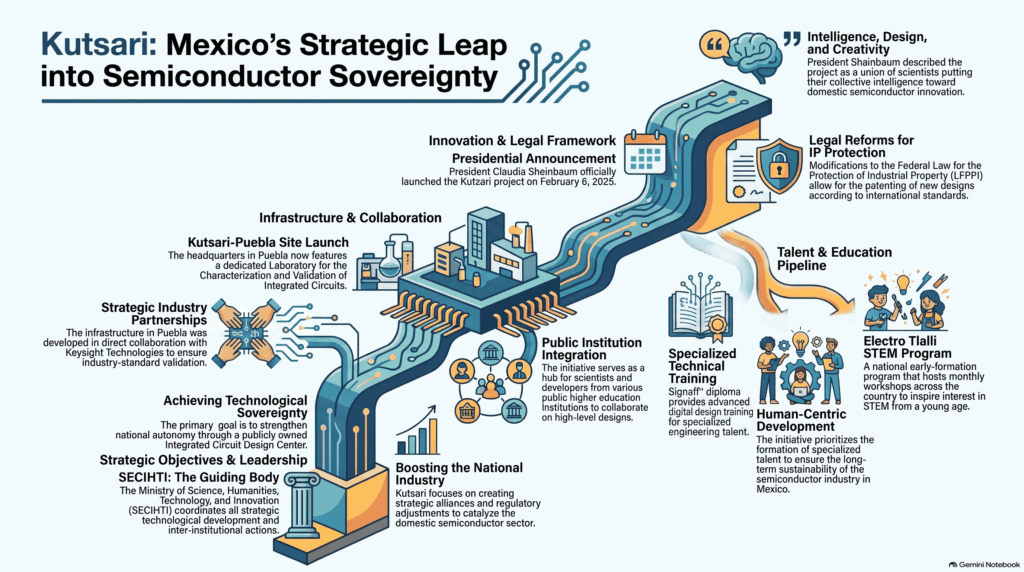
In addition, Kutsari seeks to boost the national semiconductor industry and train specialized talent.
To this end, the federal government is promoting strategic partnerships, regulatory adjustments, and the development of production and training capacities nationwide.
Within this framework, the Integrated Circuit Characterization and Validation Laboratory was inaugurated at the Kutsari-Puebla campus. In addition, this was accomplished in collaboration with Keysight Technologies.
The certificate program “Digital Design from RTL to Physical Signoff” was launched. This program aims to provide specialized training in semiconductor design. Furthermore, the “Electro Tlalli” early education program in STEM fields was implemented. It features monthly workshops at various locations across the country.
Semiconductor Design
On February 6, 2025, President Claudia Sheinbaum announced the creation of Kutsari. As a result, Mexican scientists from public institutions of higher education will be able to develop new semiconductor designs. These designs can be patented in accordance with international standards that protect innovation. This is based on amendments to the Federal Law on the Protection of Industrial Property (LFPPI).
“The Kutsari Semiconductor Design Center, or Project Kutsari: National Semiconductor Design Center, is a collaboration among many scientists and technology developers from public institutions of higher education, who will contribute all their intelligence, design expertise, and creativity to generate new semiconductor designs,” Sheinbaum said at the time.